Imagine making a virtually unbreakable flatscreen TV the thickness of a sheet of paper. An improved understanding of materials at the atomic scale allows scientists to prepare two-dimensional materials, lighting a potential path for developing such futuristic technologies. The phrase “two dimensional material” may conjure up an image of the page on which this article is printed, but a sheet of paper is actually a mess of fibers thousands of atoms thick. In a truly 2D material, atoms are connected in a single plane—giving rise to novel optical, electrical, and mechanical attributes.
One of the most touted 2D materials is graphene, a one-atom-thick sheet of carbon arranged in a honeycomb lattice. Graphene is an excellent electrical conductor, is tougher than steel, and has strong interactions with light. But even a wonder material has limitations, and scientists are actively exploring the physical properties of other exotic systems—nitrides, dichalcogenides, topological insulators, and more—as candidate 2D materials. In this sphere, the scientific communities of UC Berkeley and Lawrence Berkeley Laboratory have been a hub for applying the principles of nanoscale engineering toward theoretical and experimental study of 2D materials.
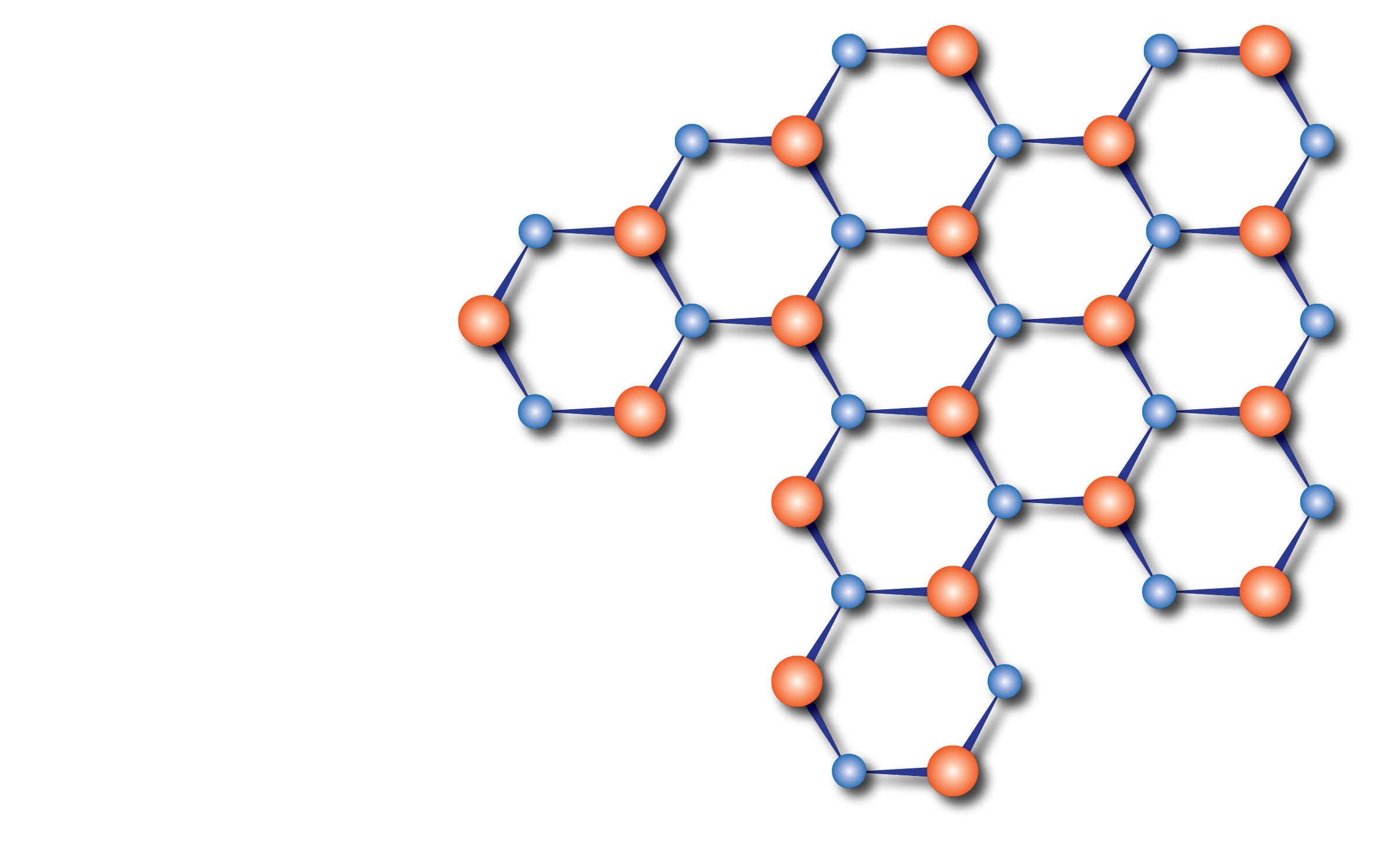
UC Berkeley professor Xiang Zhang leads the X-Lab, which has been at the forefront of a suite of high-impact studies investigating the optical and electrical behavior of nanoscale systems with confined dimensionality. Zhang’s research focuses on the 2D properties of a dichalcogenide called molybdenum disulfide. This flexible material, a viable successor to silicon for electronics because of its high and switchable conductivity, can be synthesized as stable, free-standing 2D crystals. These samples, commonly known as flakes or monolayers, are promising building blocks for nanoscale devices.
The X-Lab recently reported in the journal Nature Nanotechnology a significant advance toward understanding the nanoscale properties of molybdenum disulfide. Working with one-atom-thick molybdenum disulfide crystals and employing delicate instrumentation, Zhang’s team explored the material’s ability to convert mechanical stress and strain into electricity, a property known as piezoelectricity. Fundamental understanding of piezoelectricity in nanoscale systems establishes a framework for designing energy-efficient, flexible electronics. The applications of a viable, nanoscale piezoelectric material range from bioelectronics to logic gates for ultrafast computing.
Discovering and making piezoelectric nanoscale materials is a challenging experimental endeavor, because materials often behave completely differently when isolated in 2D. Large crystals of molybdenum disulfide exhibit no piezoelectricity because these structures have an even number of atomic layers. In such systems, atomic layers are stacked in opposite directions, and the distribution of electric charges cancels out. The X- Lab’s work was motivated by the theoretical prediction that nanoscale molybdenum disulfide crystals prepared with an odd number of atomic layers will exhibit piezoelectricity. They experimentally examined the piezoelectricity of a known number of atomic layers by balancing a single 2D molybdenum monolayer across a support that allowed for tandem electrical and mechanical measurements.
While the X-Lab’s manuscript was under review and published on arXiv.org, another paper on piezoelectricity in molybdenum disulfide was published in the journal Nature by an independent team of researchers. The X-Lab’s effort was distinguished by their approach to perform an all-in-one measurement on individual monolayers: both piezoelectric measurements and absolute validation of the number of atomic layers were performed on a single flake.
Looking ahead, developing a device using 2D molybdenum disulfide or another 2D material will have to address current technological limitations. Specifically, isolating and purifying large amounts of high-quality material will not be easy. To provide a sense of the timescale required for such developments, strategies to affordably access gram-scale quantities of graphene are emerging this year, over 12 years after flakes were first isolated from strips of Scotch tape. While large-scale production of molybdenum disulfide remains a challenge, studying its fundamental physical properties is an area rich with the potential for scientific discovery. For molybdenum disulfide in particular, the X-Lab is exploring exciting opportunities in the cutting-edge field of valleytronics, where information is encoded in the quantum properties of electrons darting through these remarkable 2D materials.
This article is part of the Spring 2015 issue.