Each year, we expect the latest generation of smartphones to offer enhanced speed and performance. These enhancements are primarily made possible by increasing the number of transistors in electronic devices. Transistors are small semiconductor devices that serve as the fundamental physical units of computation in electronics. They consist of channels of silicon implanted with atoms, such as gallium or arsenic, that change the local electrical properties. Collections of intricately connected transistors work together to perform all the
operations on your phone. More transistors mean more simultaneous computations and thus, a faster device. Today’s smartphones contain around 460 billion transistors and can perform hundreds of billions of operations every second.
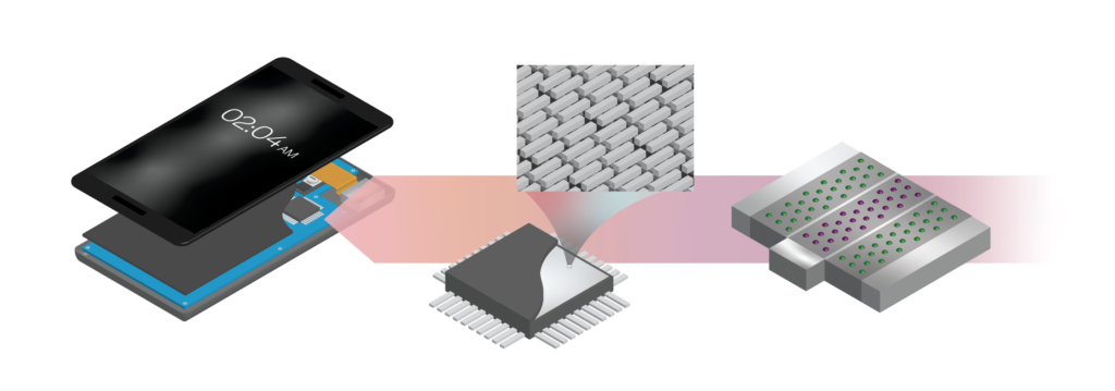 (Right) A single transistor consists of channels of silicon implanted with atoms. (Center) A microchip consists of arrays of transistors and the intricate three-dimensional circuitry that connects them. (Left) Hundreds of billions of operations performed by microchips each second enable the functions of electronic devices. Image Design: Gautam Gunjala
To improve performance, engineers must cram an ever-increasing number of transistors onto a chip that remains the size of a postage stamp. This feat is possible due to advancements in photolithography, a process by which a stencil for the circuitry of a microchip—known as a photomask—is optically imaged onto a silicon wafer. The silicon is coated with a layer of photoresist, a material that is chemically modified by exposure to light. The exposed photoresist can then be selectively removed, revealing channels of silicon that are implanted with atoms. After implantation, the remaining photoresist is washed away. Numerous iterations of this procedure produce a complex three-dimensional network of circuitry on a chip. Significant worldwide effort goes into optical improvements that enable smaller, narrower channels, thus reducing the size and increasing the speed of transistors, and allowing more of them to be patterned onto a single chip.
Major advances in photolithography have enabled a continuous downscaling of transistor size for the past 50 years, resulting in the 50 nanometer-wide transistors found in today’s electronics. However, further reduction will require still greater innovation because limitations imposed by material properties and the optical resolution limit play an increasingly
daunting role. One such innovation is a transition to extreme ultraviolet (EUV) light—a class of X-ray radiation—to transfer finer photomask patterns to silicon. Through collaborative efforts between Lawrence Berkeley National Lab, UC Berkeley, and industrial partners over 27 years, researchers have used EUV photolithography to produce features on silicon as small as 8 nanometers—a size comparable to the width of a strand of DNA.
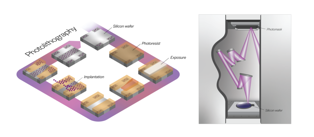 (Left) A single iteration of the photolithography process, in which photoresist that is exposed to light is chemically eroded, allowing selective implantation of atoms into silicon. (Right) An EUV photolithography system — known as a stepper — contains a reflective optical system to shrink and transfer photomask patterns onto the wafer in the exposure step. [Image Design: Gautam Gunjala]
Because EUV light is absorbed by air and traditional glass lenses, transitioning to EUV requires performing the entire photolithography process in vacuum and only using reflective optical components. As a result, the machines now being used to perform EUV photolithography are among the most complex systems ever assembled. After over 20 years of meticulously refining these systems, the first chips manufactured using EUV photolithography have appeared in smartphones this year.
The realization of EUV photolithography gives us a promising path toward the reduction of transistor sizes over the next decade. This progress—and the enhanced smartphone performance we enjoy as a result—may continue steadily until faced with the inevitable hurdles of working at an atomic scale, but for now, there is still plenty of room to shrink.
This article is part of the Spring 2020 issue.